Twenty Three Hundred
Architecture and Organisation
Dr Charles Martin
Semester 1, 2022
Admin Time
Assignment 2 due Sunday 22/5/2022 23:59 AEST
Lab 11 starts tomorrow – keep going to labs!
Lab Pack 4 due: Wednesday 1/6/2022 23:59 AEST (day before exam period)
Week 11: Architecture
What is a computer again?
Outline
A basic computer…
Don't we need more stuff?
Don’t we need more stuff?
Origins
The Z1 (1937)
created by Konrad Zuse
first digital computer: relays, programmable via punch tape, 1 Hz clock, 64 words of memory @ 22-bit, 2 registers, floating point unit, weight 1 ton
image from ComputerGeek, CC BY-SA 3.0
Z3 (1941)
first freely programmable (Turing complete) computer, relays, 5.3 Hz clock
image from Venusianer, CC BY-SA 3.0
ENIAC (1945)
ENIAC: first Turing complete vacuum-tube computer, 100 kHz clock, weight 27 tons, size 167 sq m
image from U.S. Army Photo, public domain
… then came the microbit
(not really)
Architectures
Harvard architecture
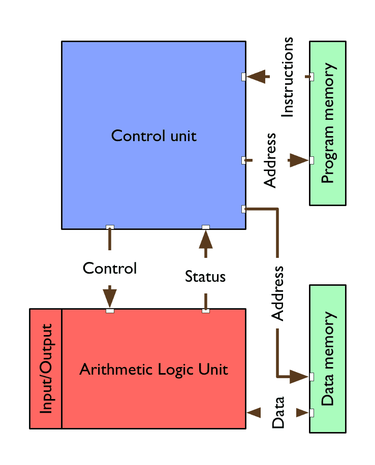
control unit concurrently addresses program and data memory and fetches next instruction—controls next ALU operations and instruction based on ALU status
Arithmetic Logic Unit (ALU) fetches data from memory, executes arithmetic/logic operations, and writes data to memory
separate memory for program & data
von Neumann architecture
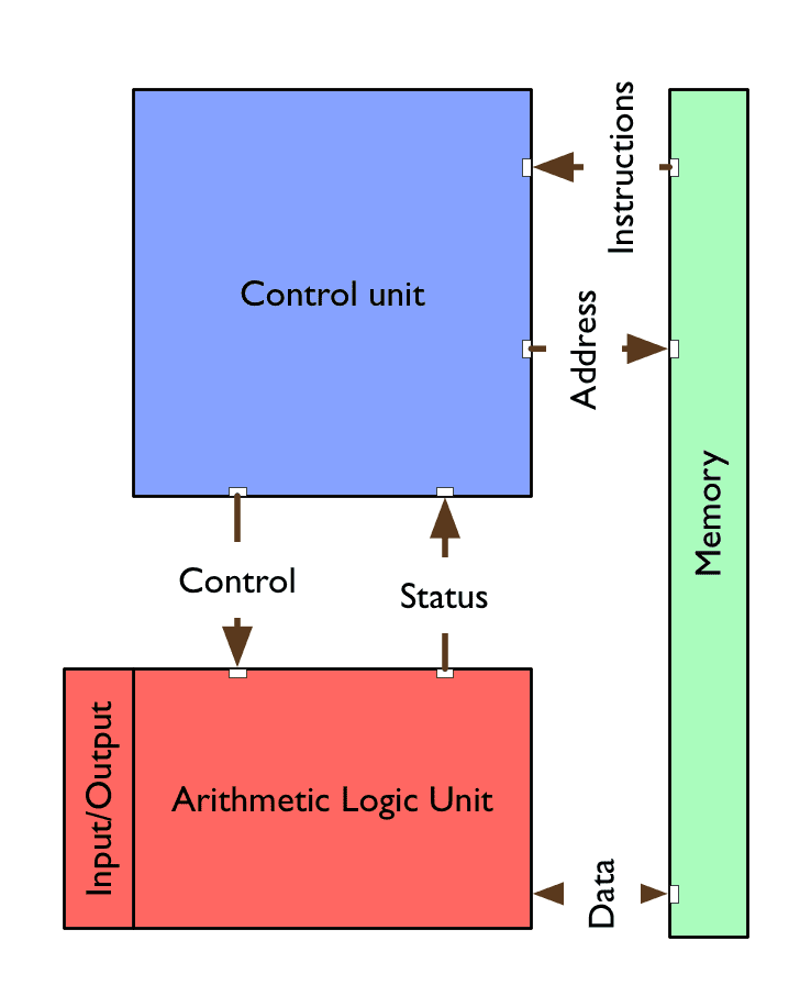
control unit sequentially addresses program and data memory and fetches next instruction—controls next ALU operations and instruction based on ALU status
Arithmetic Logic Unit (ALU) fetches data from memory, executes arithmetic/logic operations, and writes data to memory
program and data memory not distinguished (so programs can change themselves)
A simple CPU
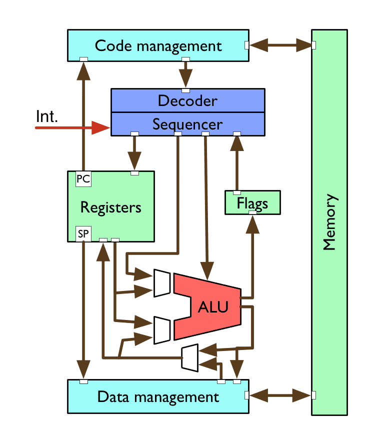
decoder/sequencer converts instructions into CPU control signals
arithmetic logic unit (ALU) performs maths & logic operations
registers provide small, fast storage to the CPU
flags indicate the states of the latest calculations
code/data management for loading/storing, caching
memory
Pipeline
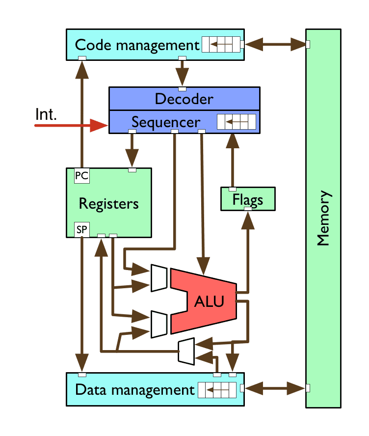
some CPU actions are naturally sequential (e.g. fetch-decode-execute).
an instruction pipeline allows these sequences to be overlapped in time
same latency, but higher throughput
Simple Pipeline
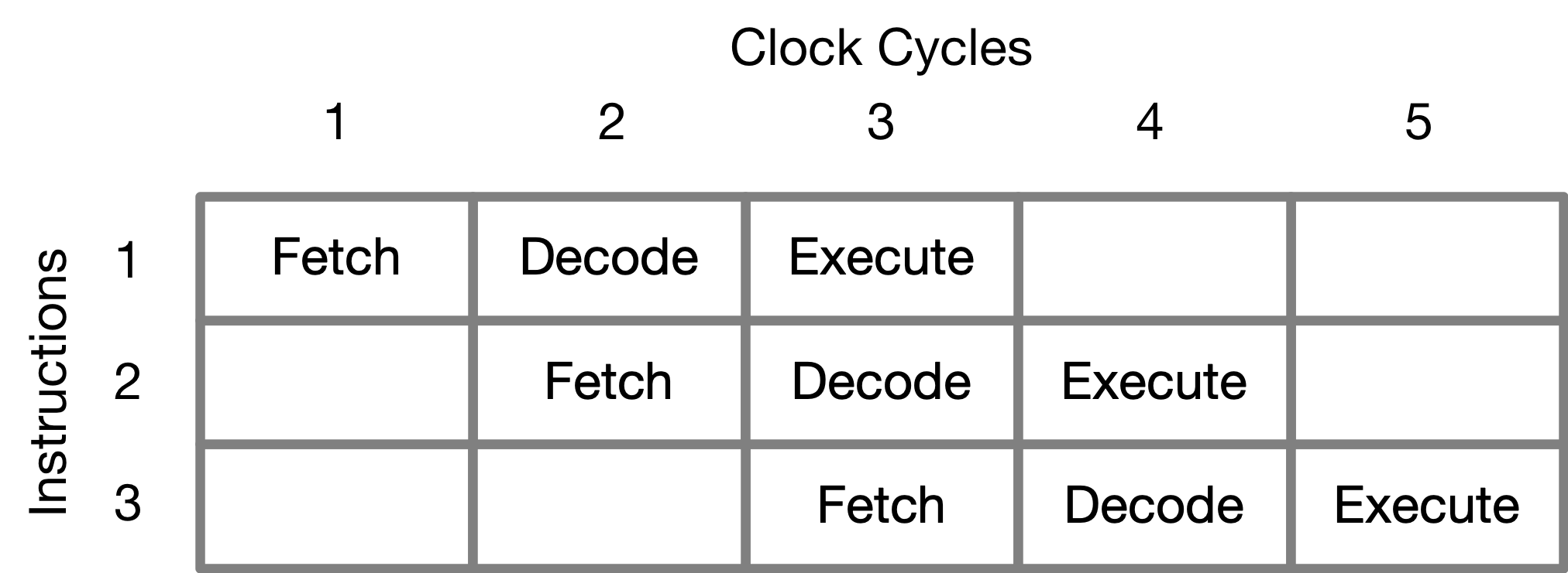
Pipeline example
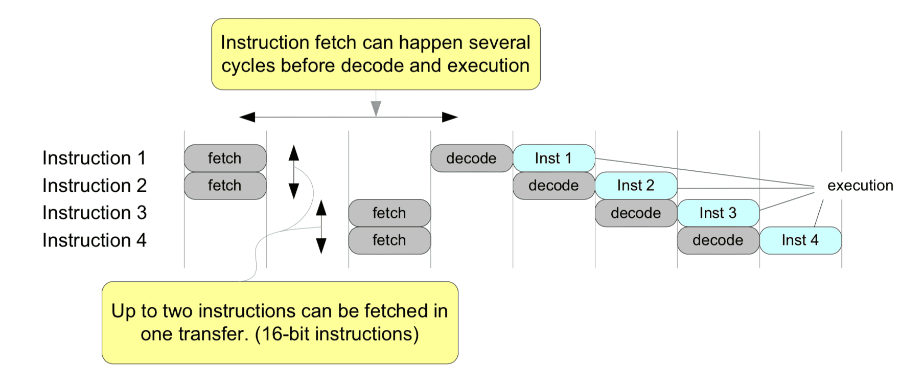
(from p15. ARM Cortex-M Programming Guide to Memory Barrier Instructions)
(conditional) branches might break the pipelines (requiring a “flush”).
Pipeline Hazards
- Hazards are circumstances that prevent the pipeline from working efficiently.
- Data: When the outcome of one instruction is required to execute the next.
- Structural: When part of the CPU hardware required by two instructions simultaneously (e.g., memory to fetch and store simultaneously).
- Control: When the location of the next branch is unknown until an instruction is executed.
How do you deal with these?
- Add “bubbles” in the pipeline?
- branch prediction?
- out-of-order execution?
- all these have downsides
Out-of-order execution
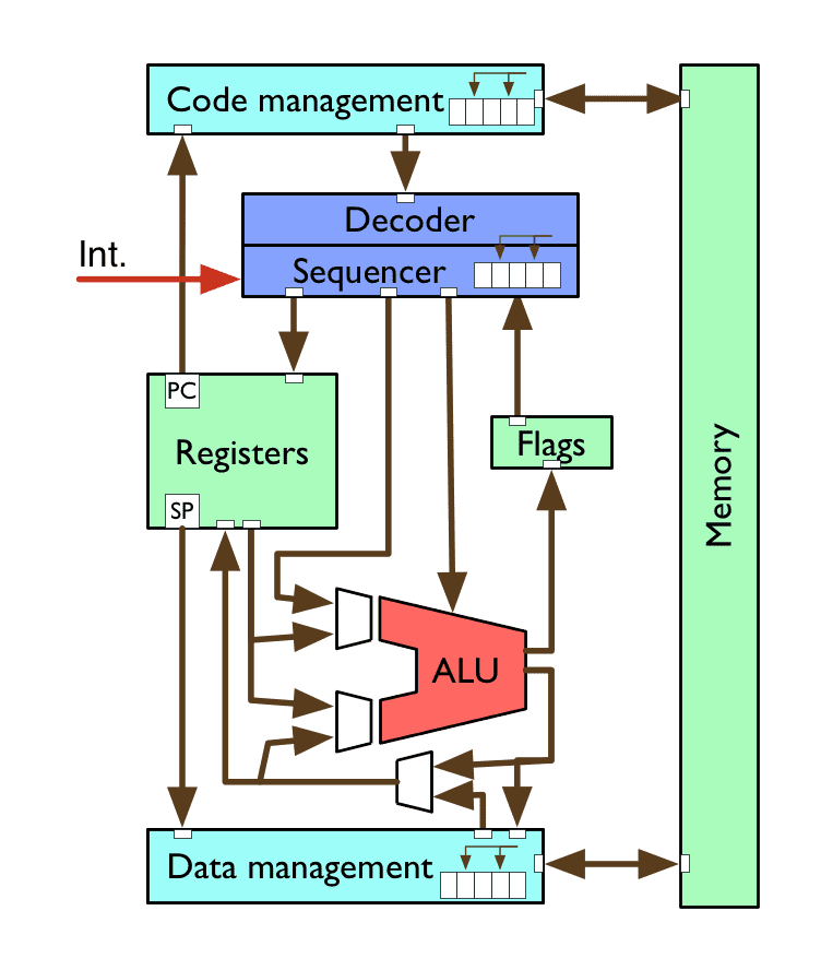
re-ordering the sequence inside each pipeline leads to ‘out of order’ CPU designs
pipeline becomes a hardware scheduler, and results need to be “re-sequentialised” (or possibly discarded)
finer-grained sequences can be introduced by breaking CPU instructions into micro code (better if there are more independent instructions)
Out-of-order example
$ f(a, b, c) = (a + b) \times c $
@ in-order
ldr r0, =0x20000000
ldr r1, [r0] @ load a into r1
ldr r2, [r0, 4] @ load b into r2
ldr r3, [r0, 8] @ load c into r3
add r1, r1, r2  @ add a and b
mul r0, r1, r3  @ (a + b) * c
@ out-of-order
ldr r0, =0x20000000
ldr r1, [r0]
ldr r2, [r0, 4]
add r1, r1, r2  @ these two are
ldr r3, [r0, 8] @ switched around
mul r0, r1, r3
Computerphile has a more detailed explanation
it's not quite magic, but...
Multiprocessing
SIMD/vector processing
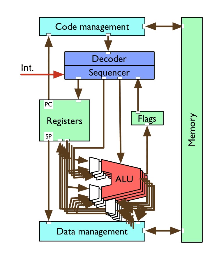
Single Instruction Multiple Data ALUs provide the facility to apply the same instruction to multiple “datas” concurrently
often requires special “wide” registers and new instructions (e.g. fitting 4 32-bit values into one 128-bit register, then adding them all using one SIMD instruction)
requires specialised compilers or programming languages with implicit concurrency
examples: NEON, Altivec, MMX, SSE2/3/4, AVX
Hyper-threading
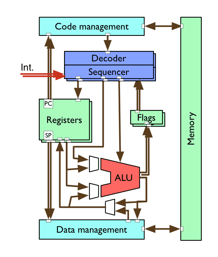
emulates multiple “virtual” CPU cores by replicating:
- register sets
- decoder/sequencer
- flags
- interrupt logic
while sharing other resources like the ALU, data management
examples: Intel Core i-series, POWER9 (up to 8 threads per core)
talk
what sort of workloads would benefit from SIMD? how about hyperthreading?
Multi-core CPUs
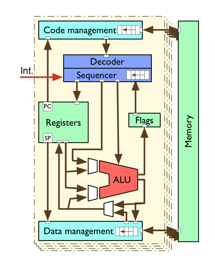
full replication of multiple CPU cores on the same chip package
often combined with the other techniques discussed
cleanest and most explicit implementation of concurrency on the CPU level
requires synchronised atomic operations, and programming languages with implicit or explicit concurrency
Flynn’s Taxonomy (1966)
Classification system for processor functionalities:
| single data | multiple data | |
|---|---|---|
| single instruction | SISD - uniprocessing | SIMD (SSE, NEON) |
| multiple instruction | MISD? (??) | MIMD (multi-core processors) |
Which of these are common today?
Amazing parallel computers of today
Your phone!
ARM big.LITTLE architecture
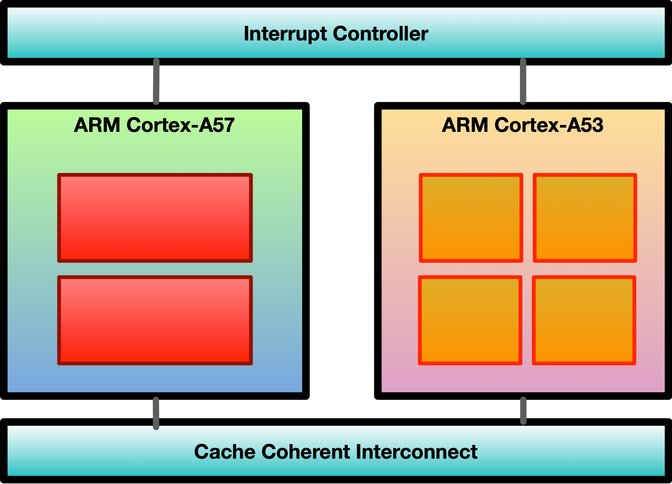
Heterogeneous computing architecture
“little” cores: efficient and power saving (use these most of the time)
“big” cores: powerful but power-hungry (use these just in bursts)
all cores have access to same memory regions
scheduler figures out where to execute threads
e.g., Apple A11 (2 big cores, 4 little)
Your gaming PC!
NVIDIA GPU architectures
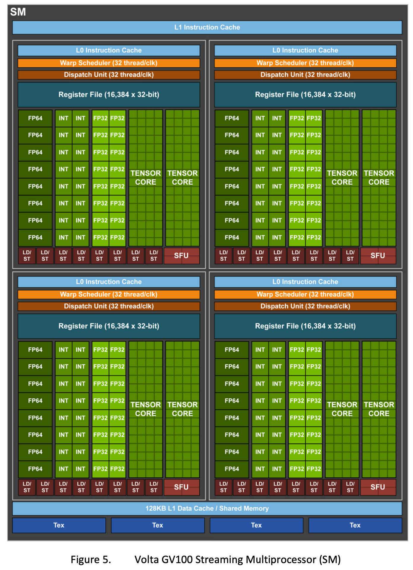
GPUs are highly parallel processors
focussed on bandwidth, not latency
NVIDIA uses CUDA (computer unified device architecture).
One CUDA SM (streaming multiprocessor) has lots of cores (~ALUs)
Image: Copyright NVIDIA.
NVIDIA Volta Architecture (V100) layout
One GPU has lots of SMs! RTX 2080 ti = 68 SMs, Tesla V100 = 84 SMs! (5376 cores!)
Image: Copyright NVIDIA, more resources
Alternatives?
Digital Computing in Plastic!
Parallax Propeller
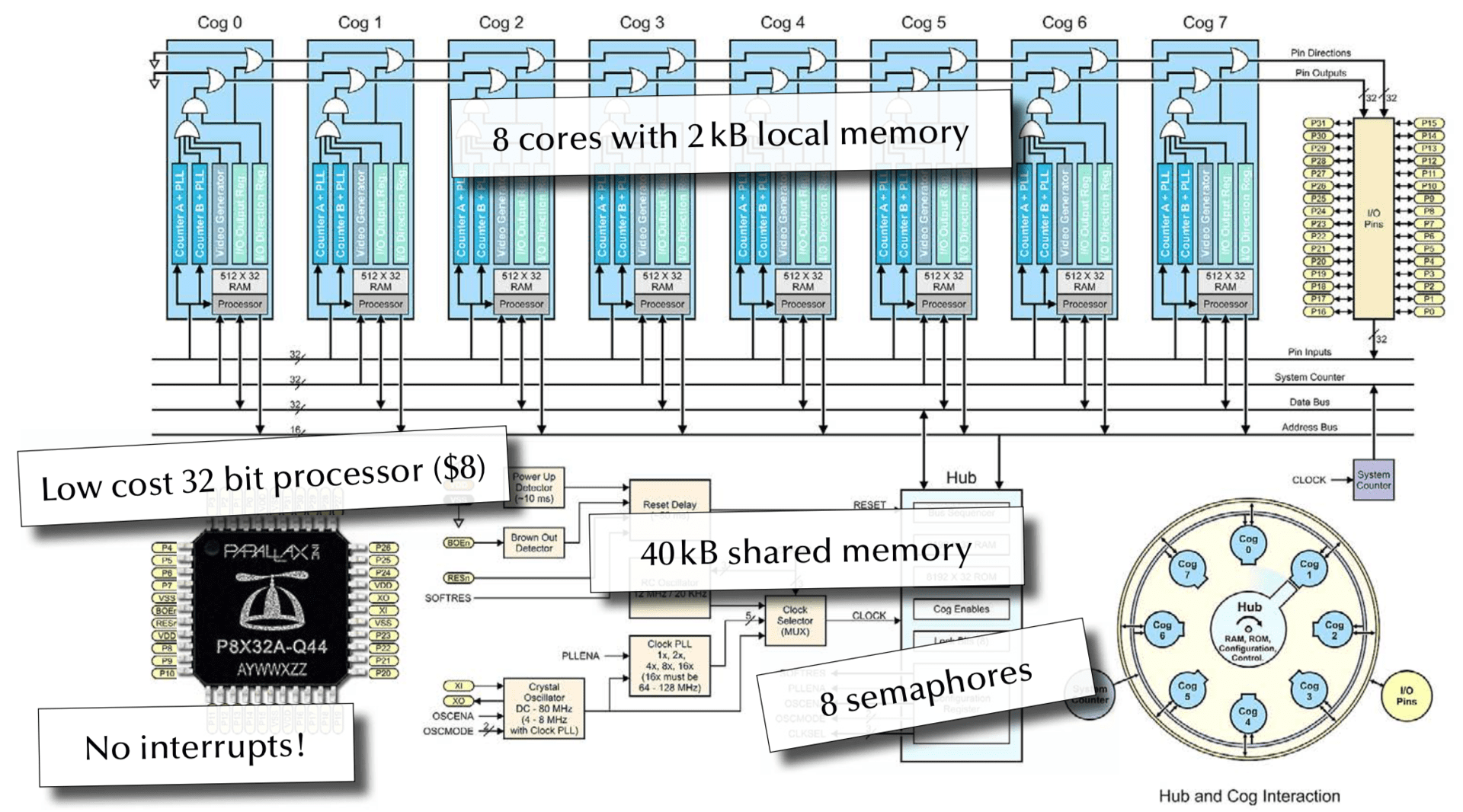
Embedded Programming without Interrupts
RISC-V

The Free and Open RISC Instruction Set Architecture
a collaborative design effort
small core ISA with lots of optional “extensions” (e.g. floating point, SIMD/vector ops)
this allows it to scale from embedded to HPC (in principle)
Intel x86/amd64?
Visual ARM1 simulation
ARM1 chip (created in 1985) is the ancestor of all smartphone chips, and also the microbit
check out this visual ARM1 simulation (runs in the web browser)
also see Ken Shirrif’s explanation
do you (kindof) get it?
Replica 1 Demo!
Replica 1 Demo
Let’s have a look at an Apple I… replica! (1975)
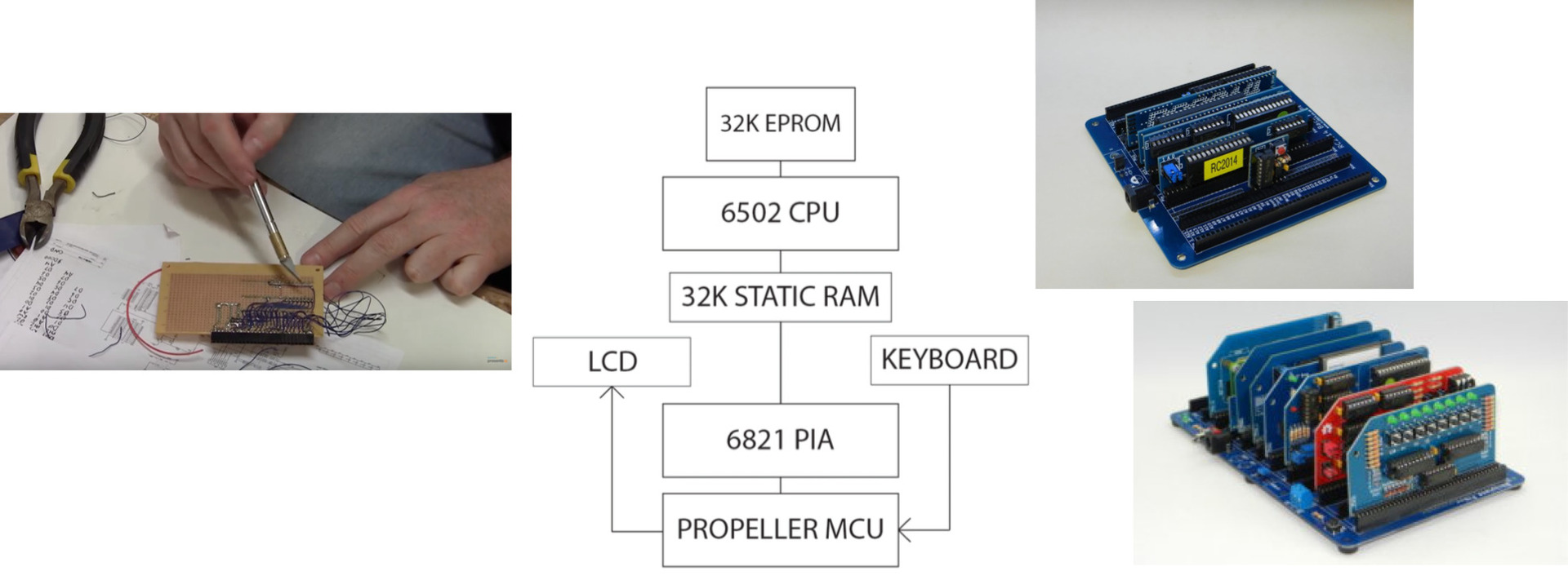
- modern replica of Apple I computer
- Serial Programming
- No OS (has a “monitor” program and BASIC interpreter in ROM).
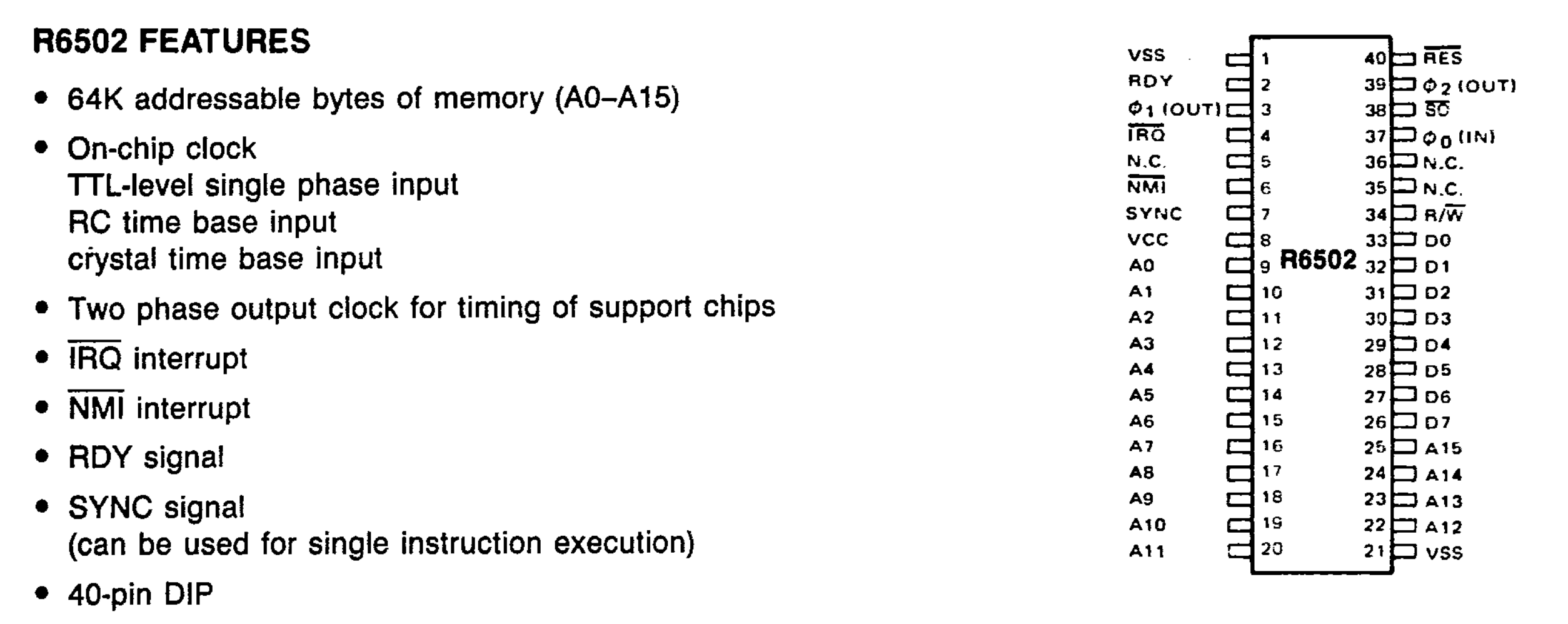
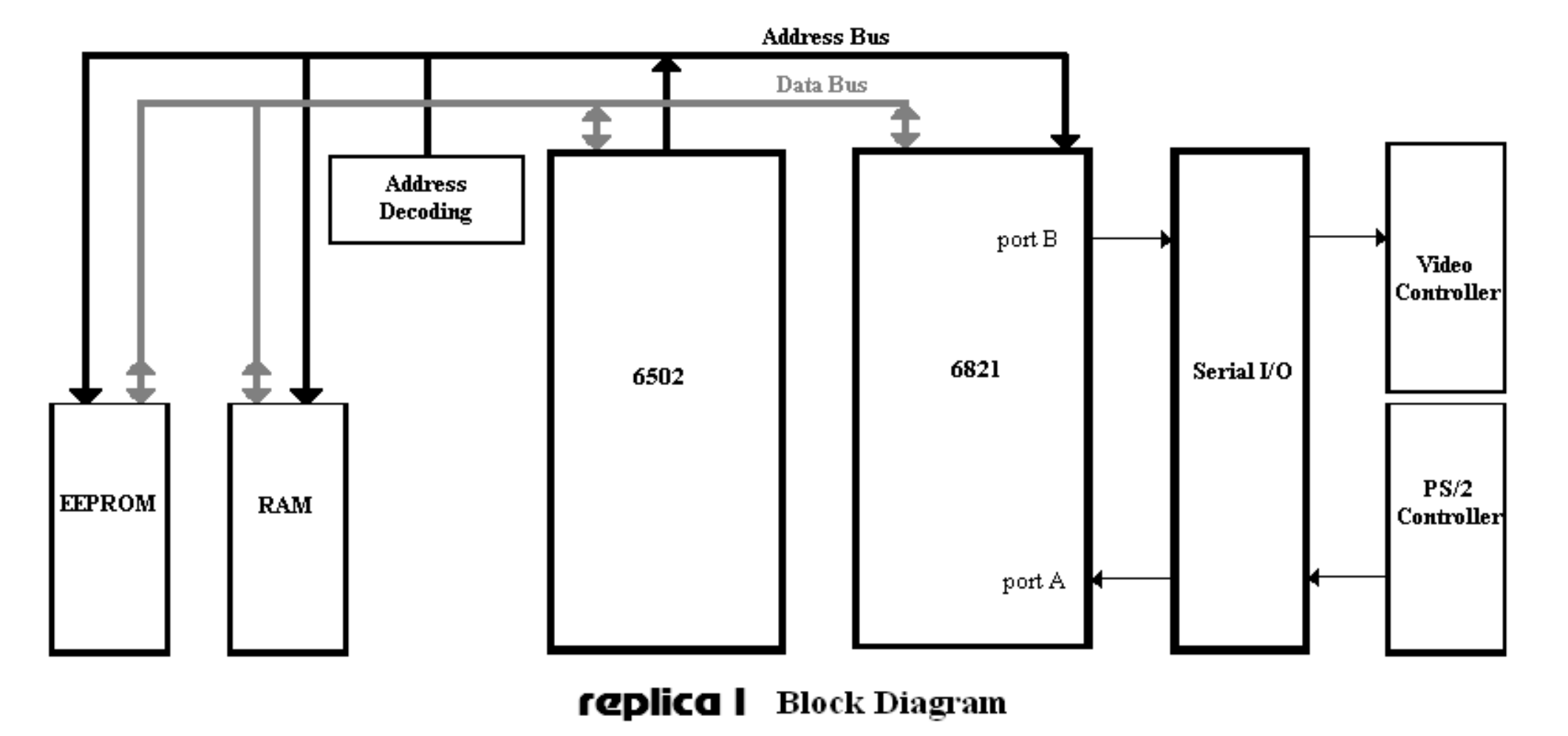
- MOS6502 processor, 6821 peripheral interface adapter (PIA), one bank of RAM, one ROM
- Modern things: USB serial adapter, Parallax Propeller (drives video and manages keyboard).
Make your own?
- Ben Heck Apple 1 Replica Build
- Get parts from AliExpress/Ebay, grab a soldering iron and start hacking!
- Alternative–Z80 computer with a “new” design: RC2014
- Build computer just from logic gates?
Further Reading
Essentials of Computer Organisation and Architecture (Null) - Ch. 1.9
Essentials of Computer Organisation and Architecture (Null) - Ch. 1.10
Essentials of Computer Organisation and Architecture (Null) - Ch. 1.11
Essentials of Computer Organisation and Architecture (Null) - Chapter 9
GPU Topics Multicore and GPU Programming